
Transmission electron microscopy can be used to image very thin slices (less than 100nm thick) of a sample with even better resolution than scanning electron microscopy (SEM). Whereas in SEM the electron beam scans across the surface and surface level information is gathered, in TEM the full electron beam is transmitted through the sample. An image is then formed from the transmitted beam, which can be used to analyse the microstructure in much greater detail than other microscopy methods.
Figures
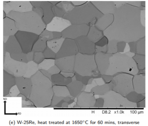
Figure One: W-25Re, heat treated at 1650oC for 60 mins, transverse (Heymer, 2020)