
Scanning electron microscopy can be used to achieve high resolution imaging of very small surfaces. An electron beam scans over the surface of the sample, and the interactions that occur between the electrons and the sample produce information about the topography and composition.
In the M4X group, SEM is used to produce detailed images of the topography, phase and composition of the superalloys produced. This allows us to examine the grain structure, composition changes across grain boundaries, and secondary phase particles in the microstructure; all of which have effects on the mechanical properties of the alloy.
To obtain information about the topography of the sample, Secondary Electron (SE) imaging is used: Secondary electrons are a result of near-surface inelastic interaction between the atoms and the incident electron, and therefore provide information about the sample surface. The secondary electron information is recorded by placing a detector into the electron chamber at an angle, so as to optimise the intensity of the beam detected. Before detetction, the electron beam is converted to a light beam by attacting them to a positively-charged Faraday case, in which sits a scintillator. The scintillator accelerates such that they present at a photomultiplier as light, allowing their signal to be amplified before detetction.
For information about the composition of the sample, Back-Scatter Electron (BSE) imaging may be used – BSE electrons originate from an elastic interaction between the incident beam and a large volume of the sample. Compositional data is obtained by consideration of the scattering angle of the BSE electrons, as this angle is proportional to the atomic number of the atoms: a larger atom will cause a greater scatter, giving a greater signal. Therefore, the intensity of the signal provides information about the constitutional elements in different phases. The BSE information is detected by a solid state detector, which contains p-n junctions connected to two electrodes. Electron-hole pairs generated by the BSEs which escape from the surface of the sample are attracted to the positivie and negative electrodes respectively, constituting an electrical current across them – the nature of which is dependent of the amount of electron-hole pairs generated, and therefore the number of BSEs escaped. This way, the current contains information about the atomic numbers of the atoms present.
Figures
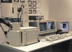
Figure One: A typical SEM instrument, showing the electron column, sample chamber, EDS detector, electronics console, and visual display monitors (source here).
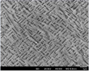
Figure Two: SE micrograph of an aged FeNiAl-Mn sample, from JEOL 6060 SEM.
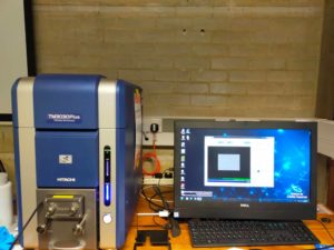
Figure Three: Hitachi 3030+ Benchtop SEM (this apparatus is commonly used for a quick overview of the SE and BSE data for characterisation. More sophisticated SEMs may be used for greater detail.